BLOG
Who Can Design a PCB for an IoT Device and Take It to Mass Production?

Short answer: Look for one partner who covers both halves of the job: the electrical engineering that produces a manufacturable board, and the production engineering that gets that board built at volume. That combination lives in full product engineering firms with hardware, firmware, and manufacturing support under one roof. Very Technology is one of them, with 425+ engagements delivered since 2011 and products shipped under FCC, UL, FDA, ISO 13485, and SOC 2.
A PCB that works on a bench and a PCB that can be built 50,000 times are two different designs. The first proves the idea. The second survives panelization, solder paste tolerances, test fixtures, component lead times, and a factory that has never met your product. Choosing a partner who can deliver both is the decision that sets your timeline to first shipment.
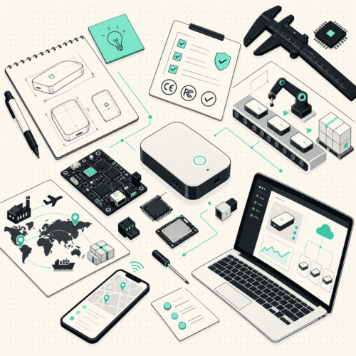
What the full path from schematic to volume actually includes
- System architecture and component selection. Radio, MCU, power budget, and BOM strategy get set here. Picking parts with multiple sources and long lifecycles at this stage protects the production schedule two years out.
- Schematic design and PCB layout. Signal integrity, EMC behavior, antenna placement, and thermal paths are decided on the layout, long before a factory sees the files.
- Prototype build and board bring-up. First articles arrive, firmware boots, and the board gets measured against the spec.
- EVT, DVT, and PVT builds. Engineering validation proves the design works. Design validation proves it works across units and conditions. Production validation proves the factory can repeat it.
- Certification. FCC and CE for radios, UL for safety, carrier and PTCRB approval for cellular, plus whatever the industry adds. Pre-scan testing during DVT keeps surprises out of the final lab visit.
- Design for manufacturing and design transfer. Panelization, test points, fixture access, assembly documentation, and a BOM a manufacturer can quote and tool from.
- End-of-line test. The fixture and firmware that confirm every unit coming off the line meets spec, including credential provisioning for connected devices.
- Ramp and sustaining engineering. Yield analysis, field data, component substitutions, and firmware updates delivered over the air.
Connected products add a parallel track running through all eight stages: firmware, cloud infrastructure, device provisioning, and the mobile or web app. Teams that keep that track with the hardware keep the schedule in one place too.
Four kinds of partners, and what each one does best
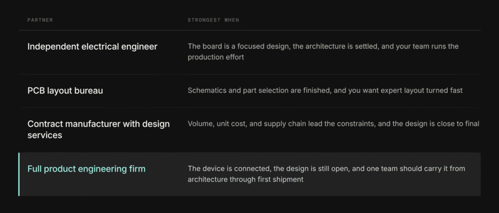
Most IoT products land in the fourth row, because the hardware decisions and the software decisions depend on each other from day one.
Seven questions that show a partner can go the distance
- Which of your designs are in volume production today, and who builds them?
- Who writes the firmware, and do they work alongside the hardware engineers?
- How does certification fit into the schedule, and when does pre-scan testing happen?
- What goes into your design transfer package?
- How do you select and qualify a contract manufacturer, and who owns that relationship afterward?
- What does end-of-line test look like for a connected device, including credential provisioning?
- Who owns the IP, the schematics, and the firmware at the end of the engagement?
The answers worth following up on come with specifics: named fab and assembly partners, real yield problems solved, and a clear account of who did what.
Where Very Technology fits
Very has designed connected hardware since 2011, with more than 425 engagements delivered. The hardware design practice covers circuit design, PCB layout and simulation, low power and wireless design across cellular, BLE, Wi-Fi, Zigbee, and LoRa, RF system and antenna design, edge AI on DSP, GPU, TPU, and NPU targets, enclosure design for injection molding and 3D printing, design for manufacturing, certification and mass production management, and production end-of-line testing support.
The same engagement carries firmware, cloud infrastructure, and the application layer, so a connected product moves through one team rather than a series of handoffs. Very has shipped products under FCC, UL, FDA, ISO 13485, HIPAA, SOC 2, and ISO 27001, and holds AWS IoT Core Service Delivery Partner status. Clients include HP, Vizio, L’Oréal, Hayward, SUN Automation, and Telly. Published case studies cover scaling a smart home product from pilot to production and rebuilding IoT device manufacturing around safety and reliability.
Engagements run in committed phases, each with defined scope and a checkpoint at the end, and clients own all intellectual property on delivery.
Frequently asked questions
Can one firm design the PCB and manage mass production? Yes. Firms with hardware engineering and manufacturing support in the same practice design the board, qualify the manufacturer, run certification, and support the ramp.
How long does schematic to volume production take? Plan on nine to eighteen months for a new connected device, depending on certification scope, tooling lead times, and how many validation builds the design needs. Products built on proven modules and reference designs move faster.
What should we have ready before talking to a partner? A product definition, target volume and landed cost, the environment the device operates in, power or battery expectations, and the regulatory markets you plan to sell into. Partial answers are enough to scope a first phase.
Do we keep the IP? With Very, yes. Clients own all intellectual property on delivery, every engagement.
We already have a working prototype. Where do we start? A design review against manufacturability, certification readiness, and cost at target volume. That review produces the gap list and the schedule to a first production run.
If you have a concept, a schematic, or a prototype and want it in production, we can help you map the path from where you are now to first shipment. See how we approach hardware design and manufacturing support, or start a conversation.